Firstly and moving beyond its 10nm SuperFin process, the naming convention of Intel’s next several die lithography will be ditching the “nm” reference. At least, that seems to be the case for the next three generations. As such, these process nodes will simply be known as Intel 7, Intel 4, and Intel 3. As per the official fluff, Intel 7 is what’s next on the roadmap, after the chipmaker’s current 10nm has run its course on the market. Previously known as the 10nm Enhanced SuperFin process, Intel says that this die lithography is expected to deliver approximately 10% to 15% more performance-per-watt (PPW) over the current 10nm SuperFin transistors, along with having more enhanced features. This includes an increased strain, lower resistance materials, novel high-density patterning techniques, streamlined structures. And even better routing with its stacks.
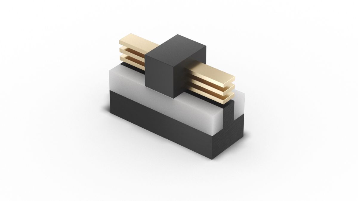
In terms of availability, Intel is forecasting production of Intel 7 to start during the first quarter of 2022. Intel 4, on the other hand, is when Intel expects to shrink its process node further, from 10nm to 7nm. Moreover, it will be the company’s first full embrace of the EUV die lithography; a technology that TSMC and Samsung are already using with their own chips. As for its performance, Intel says it will have a 20% PPW over Intel 7, with production to being during the second half of 2022, while product shipping is expected to happen the following year. Intel 3 is the last product on this list and will be the final process node that its maker says will make use of the FinFET process. Sadly, the chipmaker’s announcement about this isn’t flushed with a whole lot of detail, only that it will deliver 18% PPW over Intel 4 and that production is expected to begin in the second half of 2023. One important point to note is that all three die lithography will still actually be based on the SuperFin process, and it is only after Intel 3 will Intel move on to a brand new process altogether, with Intel 20A spearheading the charge. With Intel 20A, the company will also introduce two new “breakthrough” technology: PowerVia and RibbonFET. Starting with PowerVia, Intel says that the technology will be an industry-first implementation of a backside power delivery, which we can see via the cross-section provided. By doing this, the company says that it optimises signal routing while reducing droop and lowering noise. RibbonFET, as you can imagine, is set to be a new transistor architecture that is set to replace FinFET, which was introduced back in 2011. Like Intel 20A, there isn’t a whole lot of detail about the process, and it is likely that we will only be hearing more when the node’s production gets ramped in 2024. (Source: Intel [1] [2])